Fsae bspd test board #64
Conversation
There was a problem hiding this comment.
This resistor is too small on the 12 V LED
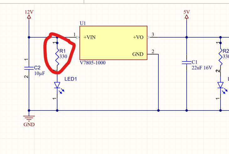
Go for something in the region of 560 Ohms to 1k
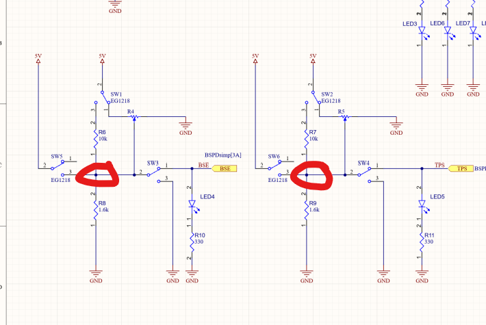
These port labels are redundant
Going through the schematic checklist
All important nets named
No spaces in net names (use underscores) (YES!)
Net names do NOT begin with numbers or other special characters such as +-/. This makes naming software variables corresponding to a certain net easier.
Consider changing the name of the 12V and 5V rail to VCC12V and VCC5V respectively.
No 4 point connections
Lots of four point connections but I think the voltage dividers are more readable in this form so no change needed.
Short circuit protection via current monitor implementation or fuse, Specifically for power rails supplying expensive parts
This board is not complex enough. No need to add scope for current monitors
No circuit compilation errors (YES!)
Active low signals have _n at the end of their net name
BSPD_OUT should technically be SC_OUT_n but I would rather we match the BSPD datasheet. If anything change it to just SC_OUT
Differential pair nets are named with _P and _N endings. Both nets in the pair should also be marked with the differential pair schematic marking in Altium (N/A)
One other comment for the schematic:
Naming these nets would make the schematic more readable
Layout Review
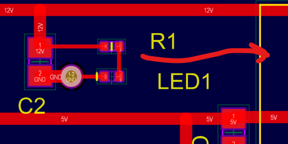
- I saw you put your name on the bottom silk. Place it on top!
- For the power supply layout, I would pull this 12V bypass cap as close to the 12V input of the regulator as possible. Also, give the LED a separate tap off the 12 V line as well as its own ground via rather than sharing one with the cap.
- Move this 5V output capacitor into the path for which we are drawing current. It has little effect all the way out to the side like this. (parasitic inductance)
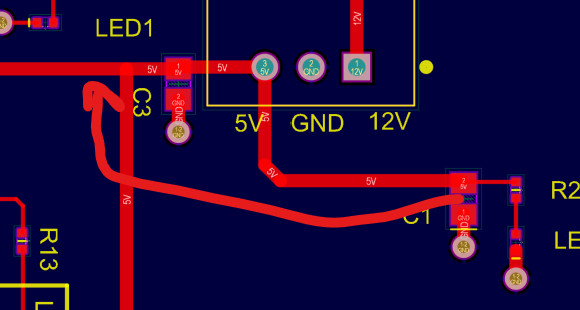
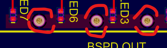
- Make this polygon taller, right now it is broken up by the vias and thermal relief lines. We want a low inductance path to the ground plane.
- This trace is still exposed in the soldermask

- Awkward shaped trace here:
- No other layout comments, ground plane looks good. It is very simple and we should not have any issues stemming from the layout.
|
|
||
| ## Brake System Plausibility Device (BSPD) | ||
|
|
||
| The BSPD is a non-programmable shutdown system with the intent to act as a fail-safe in case a vehicle’s throttle is stuck open. All Formula Society of Automotive Engineers (FSAE) teams are required to have a BSPD if their team is running an electric throttle unit. The BSPD will shut down power to the vehicle if any of the following conditions are true (FSAE 2023 Rules): |
There was a problem hiding this comment.
I think the terminology is "Electronic Throttle Control" rather than throttle unit but I am fine either way.
| @@ -0,0 +1,62 @@ | |||
| # Brake System Plausibility Device Testing Board | |||
|
|
|||
There was a problem hiding this comment.
Maybe add a quick intro here with links to the QTRONIC BSPD and datasheet PDF
|
|
||
| ### Communication | ||
|
|
||
| The BSPD Test Board has a 1x6 pin header that allows for communication to the BSPD. The tester board has three outputs TPS, BSE, and ‘BSPD_IN’ (5v), and one input ‘BSPD_OUT’. ‘BSPD_IN’ is a 5V output to the BSPD. TPS and BSE are talked about in detail in the next section. ‘BSPD_OUT’ is connected to a series of LEDs. Since BSPD_OUT is normally open (NO), the LEDs should be initially high. When the BSPD is triggered, the LEDs will transition to low. |
There was a problem hiding this comment.
Correct, Another way to summarize this is that the output (SC_OUT) is "active low". Also, SC_OUT is not normally open. The relay that gates SC_OUT is closed in working conditions (hence why the LED is on by default). By powering SC_IN with 5V we get "active low" behaviour. We could also configure the output in other ways depending on what we feed into SC_IN
|
|
||
| | SW5/SW6 | SW1/SW2 | SW4/SW3 | BSE/TPS Outputs | | ||
| | ------- | ------- | ------- | --------------- | | ||
| | P1 | P1 | P1 | 0.687V- 5V | |
There was a problem hiding this comment.
maybe note how 0.687V is computed from the voltage divider output? Kinda looks like a magic number right now. Also add a note that we got to 0.687 V by looking at the table in the datasheet and setting our pots accordingly. For this circuit to work, the threshold set in the pots should be less than 0.687 V with some safety margin. (I think it is currently 0.4V ish volts)
No description provided.