-
Notifications
You must be signed in to change notification settings - Fork 8
Adding RESET button to ispMACH 4256ZE Breakout Board
It may sound strange (especially for IT crowd :-) - but this board/circuit has no RESET pin nor RESET button. It is expected to use one of Input pins for RESET if needed.
To use this tutorial you should have working hardware and software as described in Getting started with ispMACH 4256ZE Breakout Board
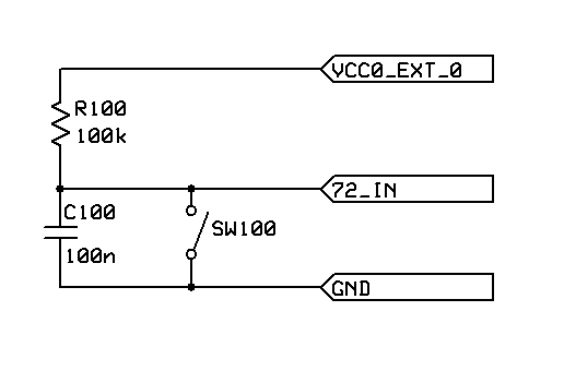
The RESET circuit is taken from Lattice Pico Development board. Schematic is as follows (I used 100 based index to avoid confusion with official Break Board schematic).:

NOTE: all signal names match PCB bottom silkscreen names.
There is nothing surprising. The capacitor C100 is used to create short RESET signal on Power-Up (and it may also help de-bouncing contacts - maybe).
Please note that this RESET signal is negative - meaning:
- logical 0 => RESET is active (button pushed, or short pulse on power-up)
- logical 1 => RESET is inactive (button released)
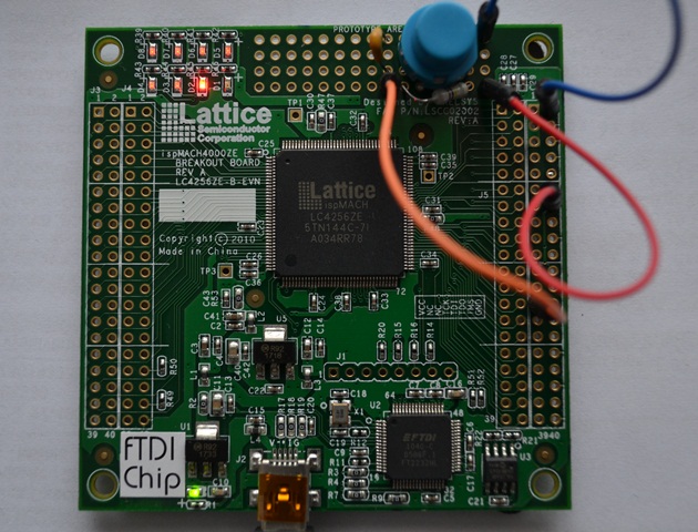
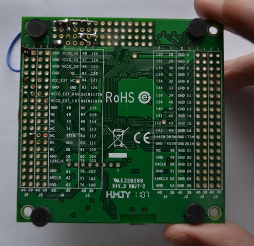
Finished Break Board with RESET button is on pictures bellow:

NOTE for wire colors:
- blue -> connected to GND (Ground)
- red -> connected to VCC0_EXT_0 (+3.3V supply - default on this board)
- orange -> connected to IN 72 pin (used for our RESET input)

Important information on Voltage:
There are two important distinct rules:
- Output pin voltage levels are hardwired by VCCO pins for Banks. The default is 3.3V and can be measured on TP1 point (for Bank0) And TP2 point (for Bank1)
- Input pint voltage is individually selectable in Constraint Editor
Summary:
- For Output pins you don't need to worry - voltage is hardwired on board
- For Input pins always verify selected voltages on Constraint Editor for each input pin
Now when we have RESET button we should test it - we shall create trivial project that would show:
- RESET state on LED D1
- inverted RESET state on LED D2
To create new project do the following:
- create initial Verilog HDL file
c:\projects\res_test.vwith this content:
// trivial RESET button test
module res_test (led,nrst);
  output [1:0] led;
  input nrst;

  assign led[0] = nrst;
  assign led[1] = !led[0];

endmodule
NOTE:
nrstis shortcut for "Negative RESET" meaning that RESET is active when logical '0' and inactive in logical '1'.NOTE2: If you are curious you should ask - how D1 works - when our RESET is negative (shouldn't also D1 invert this signal before output?).
It is very simple - attached LED D1 - D8 also use negative logic (they light when there is logic 0 on ispMach CPLD output. And so negation of negation cancel each other.
- run ispLEVER CLASSIC 2.0
- click on File -> New Project...
- Fill in:
- Project Name:
res_test - Location:
c:\projects\res_test - Design Entry Type:
Verilog HDL - Synthesis Tool:
Synplify - Simulator Tools:
Active-HDL
- Project Name:
- click on
Next - select following:
- Family:
ispMACH 4000 - Device:
LC4256ZE - Speed Grade:
-5.8 - Package Type:
144TQFP - Operating Conditions:
Commercial(the only option in my case) - Part Name (just check):
LC4256ZE-5TN144C(should be same as name of Lattice chip on PCB)
- Family:
- click on
Next - click on
Add Source...button- select file
c:\projects\res_test.v - keep "Type of Source":
Verilog Module - click on
OK
- select file
- check on
Copy Source to Work Directory - click on
Next - click on
Finishto confirm project information
Defining Input & Output PINS:
- Ensure that of "Yellow chip icon" is elected
- In Process window double-click on "Constraint Editor"
- wait a while (it will compile our Verilog HDL file first) until Constraint Editor appears
- to connect Input PIN to our RESET circuit:
- expand
res_test->Input Pins->nrst- and double-click onnrst- type
72inPincell - I/O type change to:
LVCMOS33- very important - unlike outputs (which voltage is hardwire to voltage on VCCO pin of corresponding bank) - input voltage is defined programmatically in in constraint editor! - on "Pull" select
OFF(we have our own Pull-UP resistor in RESET Circuit)
- type
- expand
- to connect output LED D1:
- expand and double-click
on
res_tests->Output Pins->led(1:0)->led_0_ - fill in:
- Pin: 71 (see
ispMACH4256ZEBreakoutBoardEvaluationKitUsersGuide.PDF"Figure 6. J1 Header Landing and LED Array Callout" to verify. - Pull: OFF (maybe not needed?)
- Pin: 71 (see
- expand and double-click
on
- to connect output LED D2:
- expand and double-click
on
res_tests->Output Pins->led(1:0)->led_1_ - fill in:
- Pin: 70 (see
ispMACH4256ZEBreakoutBoardEvaluationKitUsersGuide.PDF"Figure 6. J1 Header Landing and LED Array Callout" to verify. - Pull: OFF (maybe not needed?)
- Pin: 70 (see
- expand and double-click
on
- press
Ctrl-Sto save Constraints - return back to ispLEVER
- ensure that "Yellow chip" icon text is selected
- double-click on
Fit Designin Processes Window It should build project without errors.
Creating new project in ispVM
- run ispVM 17.9
- click on "Close" if you have opened existing project.
- click on File/New
- click on Options -> "Cable and I/O Port Setup"
- ensure that are set:
- Cable Type:
USB2 - Port Setting:
FTUSB-0
- Cable Type:
- click on OK
- press
F2to do ispTools -> Scan Chain - our
LC4256ZEshould appear - right-click on it and elect "Edit Device"
- click on "Browse..." and select existing
c:\projects\res_test\res_test.jed - click on "OK"
- click on
Ctrl-Sto save configuration - fill pathanme like
c:\projects\res_test\bboard.xcf
To programm connected Kit:
- press
Ctrl-Gto programm device = Project -> Download
If everything is OK than:
- LED D2 should be lighting
- LED D1 should be off
When button is pressed than both LEDs should Flip (D1 on, D2 off).
To simulate input (called stimulus) and output we need to create so called "test fixture". We need to:
- select source file
[res_test (res_test.v)]in "Sources in Project:" Window - double click on "Verilog Tet Fixture Template" in "Processes ..." Window
- now rename (for example in TotalCmd) generated
file
res_test.tfttores_test_tf.v - now click on Source -> Import ...
- and import file
res_test_tf.v - change Type of Source: to
Verilog Test Fixture - click on OK
- in "Associate with" you can keep highlighted our Device Name (LC4256ZE-....)
- now right-click "res_test_tf.v" in "Sources in Project" Window
- click on "Open"
- add to last
initial beginblock:
    initial begin
            nrst = 0;
        #300 nrst = 1;
        #300 nrst = 0;
end- in 300 time-units we changed nrst from 0 to 1, and after another
300 time units we change it back. By default there is timeunit
timescale 1 ns / 1 ns(= timeunit is 1ns with precision 1ns) so it does mean:- in 0ns nrst = 0
- in 300ns nrst = 1
- in 600ns nrst = 0
- Active-HDL simulate
1uSin total - so we tried to change our values evenly (only roughly :-) - save that modified file (
Ctrl-S)
Having source file "res_test_tf.v" still selected you can now try to double-click on one of available Process links:
- Aldec Verilog Functional Simulation
- Aldec Verilog Timing Simulation
There is very important differnce between these two:
- The Functional simulation does not simulate real gate delays (you can see that led output are changed immediately after nrst change)
- The Timing simulation simulate even gate delays (there is visible that led output follows nrst change).
See bellow screenshot from Timing simulation (with delays):

Now we will utilize our RESET circuit in running LED D5-D8. It uses cyclic shift register which will not work without proper initialization.
To program running light do:
- change
res_test.vto:
//  RESET button with running light on LED D5-D8 (aled)
module res_test (led,aled,nrst);
  output [1:0] led;  // two FLIP LEDs D1, D2
  output [3:0] aled; // Animated LED  D5-D8
  input nrst;        // RESET button/power-up

  reg [3:0] d; // non-inverted data for aled

  // tmr_clk is ~ 5Hz
  defparam I1.TIMER_DIV = "1048576";
  OSCTIMER I1 (.DYNOSCDIS(1'b0), .TIMERRES(1'b0), .OSCOUT(osc_clk), .TIMEROUT(tmr_clk));

  // our FLIP LEDs untouched
  assign led[0] = nrst;
  assign led[1] = !led[0];

  // animated led use inverted signal - D
  assign aled = ~ d;

  // use positive RESET in equations
  assign rst = ~ nrst;

  always @(posedge tmr_clk or posedge rst)
     begin
	if (rst)
            d = 4'b0001; // Asynchronous processing of "rst"
         else
            d = {d[2:0],d[3]}; // Synchronous processing on posedge of "tmr_clk"
     end

endmodule- do not forget to save it ->
Ctrl-S - in process Window double-click on
Constraint Editor - expand/double-click on
res_test->Output Pins->aled(3:0) @->aled_0_ - assign
61toaled_0_ - similarly assign:
- Pin
60toaled_1_ - Pin
59toaled_2_ - Pin
58toaled_3_
- Pin
- press
Ctrl-Sto save changes - in process window right-click on
Fit Designand click onStart - after successful compilation reprogram you Kit in
ispVM
After reprogram you should see that:
- LED D5 through D8 have animated light from right to left
- LED D1, D2 have retained their original functions (D1 off, D2 on)
When RESET is pressed and hold:
- animation is stopped on initial value - only LED5 i on
- LED D1 is on, D2 is off
After RESET release (or after Power Up), only LED D2 is on and LED D5-D8 are animated.
NOTE:
Verilog HDL is quite often counterintuitive: If you think that "posedge rst" means that "rst" is processed on rising edge than you are wrong.
According to BhaskerVerilog page 78, it behaves as following:
- all
if (...)onposedgeornegedgeinput parameters are processed asynchronously- implicit parameter (processed with
elseis processed synchronously.So in our example: "rst" - processed asynchronously "tmr_clk" - processed synchronously on rising edge of "tmr_clk"
Hmm - now you know why "C" of "CPLD" really means "Complex" :-)
Fix simulation...
Copyright © Henryk Paluch. All rights reserved.
